
We offer quality products and services to our customers due to our strict implementation of quality control system in each aspect of PCB assembly and Manufacturing. Inspection is a critical step in our PCB production process. Checking PCBs after each phase of the process enables us to catch flaws before moving on to the next stage, which can save further time and money on a defective product. This process helps to ensure consistent quality among your boards and assembly.
Other quality checks are:
Due to our Design for Assembly (DFA) and Design for Manufacturinf (DFM) methodologies we eliminate the process problem during the initial prototyping stage.
Nitrogen Reflow or Soldering Provides Improved soldering quality specially for Pb-Free Assembly. Higher surface tension as well as less reoxidation of IC terminals will increase the wetted surface by 20% to 30%, resulting in increasing solder joint strength. Higher surface tension minimizes solder balling when using fine pitch solder paste. Less oxidation also improves the wetting on NiAu and bare copper solder lands. Also the soldering process will be less sensitive to poor solderability and solder lands and component terminals, thereby improving the soldering BGA and CSP devices. Visual appearance of the solder joint surface will be smoother and shinier, especially for Pb-Free Assembly making it easy to inspect and rework. Larger surface tension can hold larger and heavier components on bottom side when performing double reflow.
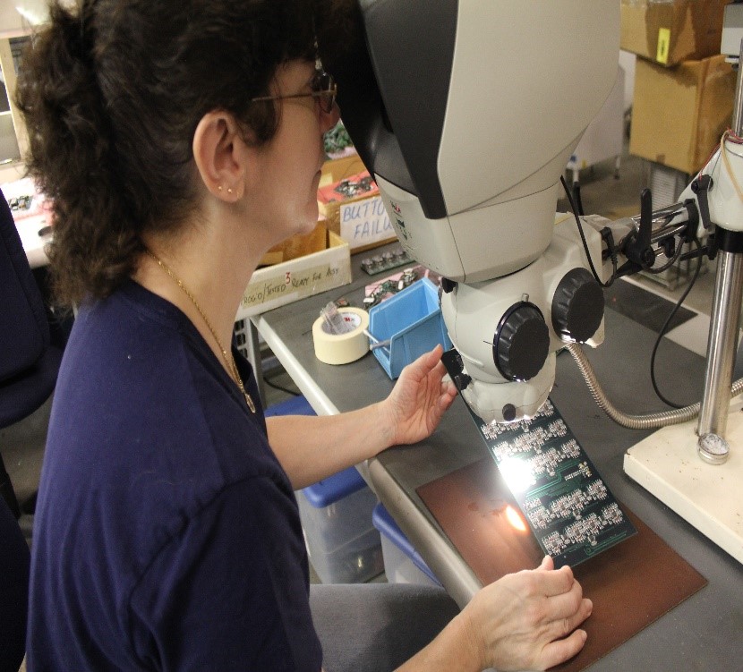
Automated Optical Inspection(AOI): AOI is an automated visual inspection methodology used primarily to test for defects in printed circuit board assemblies (PCBAs). AOI autonomously scans PCBAs with cameras and detects catastrophic failures, such as missing components, and quality failures, such as misshapen fillet or components that are skewed.
AOI works best in production environments with very high volumes and very low component variabili
X-Ray Inspection: X-ray inspection is ideal for more complex boards and offers some capabilities that other inspection methods do not, such as the ability to see through chip packages. It also works well for inspecting densely packed PCBs and allows for a more detailed inspection of solder joints. The technology is a bit newer and more complex, and it can be more expensive. It is economical only if you have a high volume of densely populated boards with BGAs, CSPs and other such packages.
Flying Probe Testing for PCB’s. Our Fabrication house will provide this service to make sure the boards are error free
An ESD and climate controlled environment is also utilized to ensure that the finished products meet all standards of efficiency, reliability, and quality
.All our processes are continually reviewed and updated per ISO requirement. We have one certified IPC Trainer and all the manufacturing staff is certified IPC Specialist.
Our printed circuit board manufacturing comply with UL safety certification, includes the UL flammability rating of 94V-0.
RoHS/WEEE Compliant – We comply with Restriction of Hazardous Substances Directive. It is Directive on the restriction of the use of certain hazardous substances in electronic and electrical equipment. We offers lead-free PCB board surface finishing and assembly processing.
Additional Certifications: IPC-600-A Certified Trainers, IPC-610-D Certified PCBA Inspectors, J-STD-001E Certified PCBA Soldering Technicians.
We strive for zero defect product. . We have in place policies, standards and procedures to reach this goal. Our Quality Control is built into each phase of the manufacturing cycle to prevent unnecessary repair or rework.
Electronic Integration has in place work instructions and procedures to ensure that the product meets the customer’s specifications as well as a high level of process repeatability. Documented processes and procedures are used to improve standard and non standard requirements.
We constantly review and rank every supplier periodically to ensure a materials are provided as per our customers requirements.
We apply Design For Manufacturability and DFT guidelines to customer’s requirements before proceeding with an acceptance of order so as to confirm customers specifications, delivery and other technical and business requisites can be met.
Electronic Integration Inc periodically conducts surveys to gather feedback both positive and negative from our customers. This in turn helps us to make improvements.
We are ISO 9001:2015 certified and our inspectors and solderers are trained and certified per IPC 610 Class 2 and 3 standards. During the production cycle different inspection methods will be performed based on customer requirements They are Visual Inspection, Xray Inspection , AOI Inspection and In circuit Testing.
We can help you with your requirements. We are ISO9001-2015 certified. We uphold to IPC standards for both performance(IPC 6012) and acceptability IPC-A-610 class 2 and class 3 for pcbs. We have Certified IPC trainer and solderers, are ROHAS, REACH and conflict material compliant, EPA,FAR and NAFTA, compliant.
At Electronic Integration Inc, we are committed to providing top-quality electronics and exceptional service to our customers worldwide. Stay ahead with our latest tech innovations.